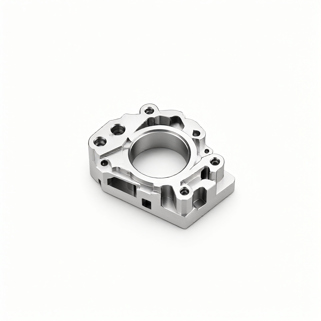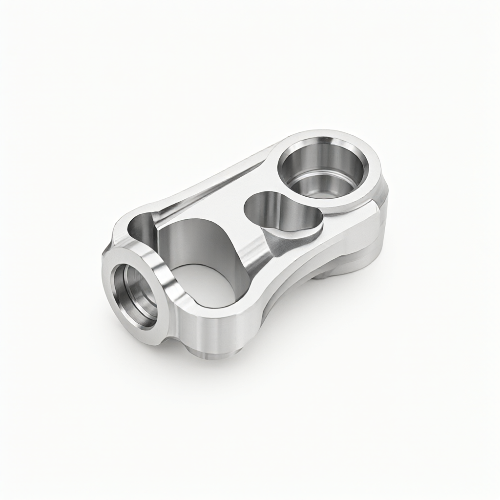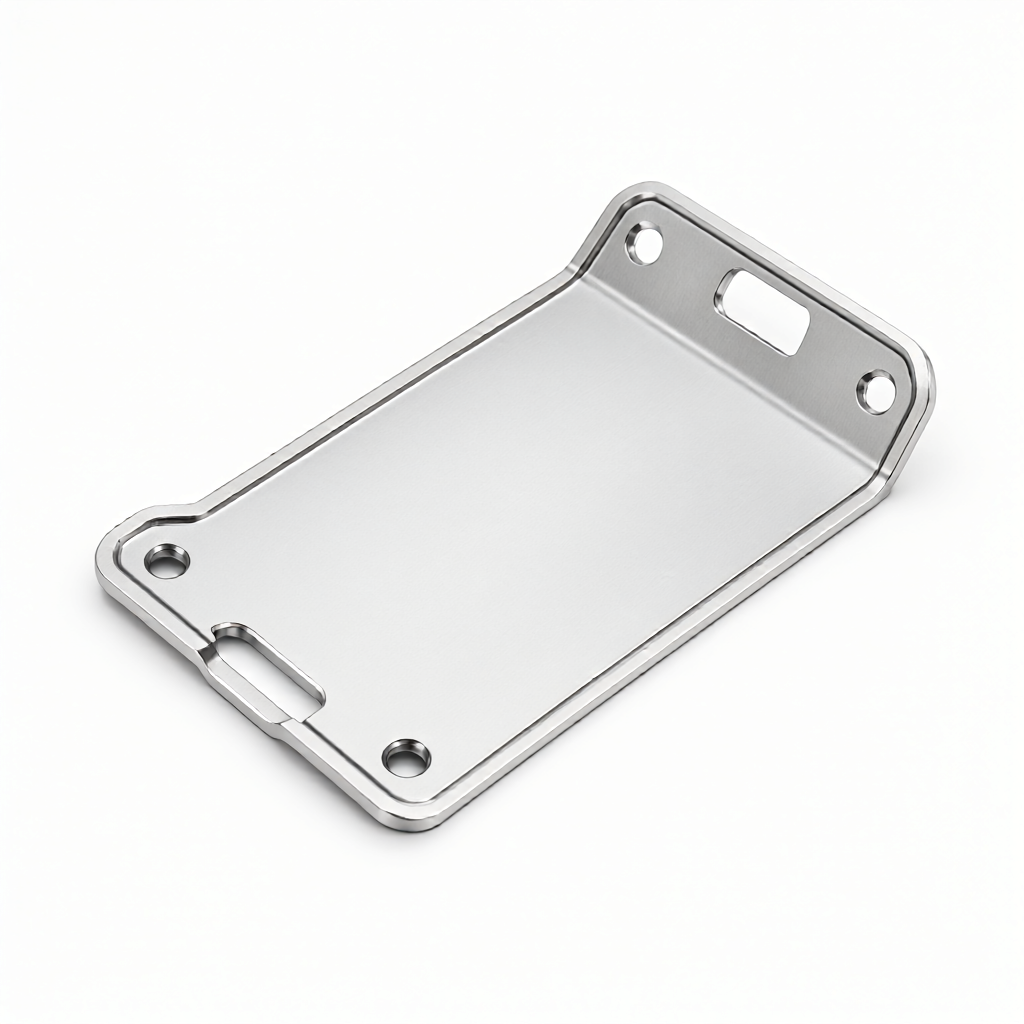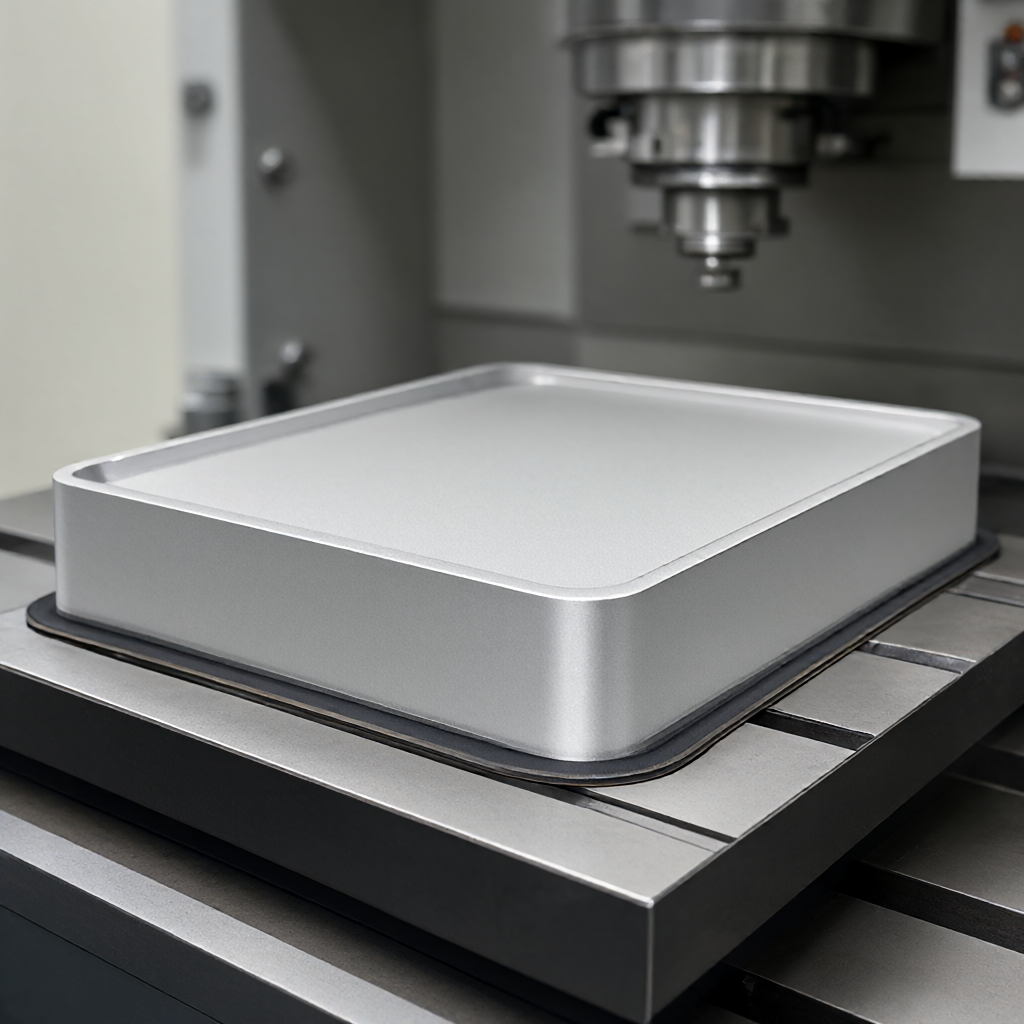


In the development of semiconductor and medical diagnostic equipment, the precision machining of microfluidic chips is the core difficulty. Traditional 3-axis milling is difficult to process wafer edge chamfers and complex curved surfaces, whileFive-axis CNC machiningThis paper will analyze how to use five-axis CNC center to complete edge chamfering, channel milling and surface finish control of microfluidic chips, covering material selection, process parameters, common failure analysis and acceptance criteria, providing technical reference for engineers and purchasers.
Core Advantages of Five-axis CNC Machining Microfluidic Chips
Microfluidic chips are usually made of silicon, quartz, glass or high-performance engineering plastics with small feature size, thin structure and tight tolerances. Five-axis machining centers (e.g., equipped with rotating axes A/C) allow the tool to always maintain a good angle with the workpiece, avoiding vibration and deformation caused by excessive tool overhang common in 3-axis machining.
- Complex Surface Milling: It can process inclined channel or spherical microstructure at one time, reduce clamping times and reduce accumulated error.
- Edge Chamfering Automation: For 100mm or 200mm wafer edges, the five-axis linkage can achieve a depth chamfer of 0.1 mm to 0.5 mm, and the sidewall roughness Ra can be controlled within 0.4μm.
- High rigidity and precision: With high-speed machine head (maximum speed 12000-24000 rpm), support carbide micro-diameter tools for high-speed milling, improve surface finish and reduce thermal damage.
For series production, 5-axis machining is more consistent than manual chamfering or traditional 3-axis side milling. DFM (Design for Manufacturing) recommendations optimize tool paths to avoid tool yield in thin-walled areas.
Process Flow and Parameter Setting for Wafer Level Machining
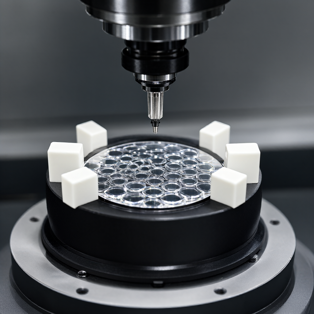
At the heart of wafer-level processing lies chuck stability and tool path planning. Wafers are usually held by vacuum chucks or custom fixtures, and five-axis machines feed tools normal to the wafer edge through C-axis rotation or A-axis tilt.
critical process parameters
- speed of mainshaftAccording to the tool diameter adjustment, micro-diameter tools (such as 0.5mm-2mm) usually need 15000-24000 rpm high-speed cutting.
- feed speed: Z-axis feed is 5-10 mm/min during rough milling, and is reduced to 0.1-0.5 mm/rev during finish milling edge chamfering to ensure smoothness.
- tool selection: It is recommended to use coated carbide end mills or miniature ball nose cutters with a diameter of 0.5-3mm and a blade length ratio L/D ≤ 3 to reduce overhang vibration.
When machining silicon wafers, special attention should be paid to the use of coolant (MQL micro-lubrication) to avoid excessive tool wear due to dry cutting. For glass or ceramic materials, diamond micro-drills or specially coated tools should be used and feed rates adjusted to suit high hardness characteristics.
Quality control of edge chamfering and surface treatment
The edge chamfering of microfluidic chips is not only to remove sharp edges and cut hands, but also for the feasibility of subsequent wafer bonding or packaging processes. The chamfer angle is usually 45° or 60°, and the depth is 0.1- 0.3 mm. The advantage of five-axis processing is that the tool posture can be dynamically adjusted to ensure a smooth transition at the chamfer root without residual flash.
Surface Roughness and Inspection
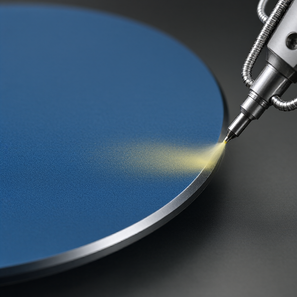
- roughness requirements: Channel inner wall Ra ≤ 0.4μm, surface flatness ≤ 2μm (for 100 x 100 mm wafers).
- detection means: Full surface scanning using optical surface roughness tester (e.g. KLA-TENcor); sampling critical feature size using coordinate measuring machine (CMM) with tolerance control of ±0.01mm.
- visual inspection: High power microscope to check the chamfer edge for chipping, scratches or sticking marks to ensure no defects.
After surface treatment (e.g. plasma cleaning, anodization or plating), surface integrity needs to be evaluated again. For microfluidic chips on aluminum alloy substrates, anodization can improve corrosion resistance, but attention should be paid to the risk of pore clogging. Thin layer oxidation is recommended for pore sizes greater than 50μm.
Comparison of material selection and cutting performance
Different materials have great influence on the performance of microfluidic chips. Silicon has excellent thermal conductivity and chemical stability, but its hardness is high (Hv 1000+) and its processing cost is high; aluminum alloy is light and easy to process, but it needs surface insulation treatment; polyimide (PI) and other polymers are suitable for flexible microfluidic, but their temperature resistance is limited.
| material trademark | Hardness (Hv) | Recommended tools | main advantage | Processing Difficulties and Countermeasures |
|---|---|---|---|---|
| Monocrystalline silicon/polycrystalline silicon | 1000-1300 | diamond/ CBN | High thermal conductivity, good biocompatibility | Cutting force, easy to break edge; need low-speed high-rigidity cutting, cooling sufficient. |
| 6061 aluminum alloy | 70-90 | Coated Carbide/High Speed Steel | Easy to process, light weight, anodized | Tool sticking risk; MQL lubrication, TiAlN coating on tools to prevent sticking. |
| quartz glass | 550-650 | diamond microdrill | High transmittance, corrosion resistance | Brittle, easy to crack; small cutting depth, more tool, avoid impact load. |
| PEEK (polyether ether ketone) | 200-300 | Cemented Carbide/Quick-change Tool | High temperature resistance, self-lubricating, medical grade | Elastic deformation is large; clamp pre-tightening is required to avoid rebound affecting tolerance. |
The choice of materials depends on the end-use scenario. For example, PEEK or quartz are preferred for medical in vitro diagnostic (POCT) equipment due to their high biological safety, while aluminum alloys or steel are preferred for semiconductor test sockets to reduce costs and ensure electrical performance.
Common Failure Modes and Avoidances
In actual processing, microfluidic chips often have the following failure modes:
- Tool Chatter: Cause ripples on the wall of the channel, roughness exceeds the standard. Avoid: Reduce the cutting depth ap, increase the tool rigidity, optimize the grip length of the tool holder.
- thermal deformation: High speed cutting generates heat, leading to thin wafer warpage. Avoid: Use micro-lubrication (MQL) or aerosol cooling to avoid thermal shock caused by large amounts of cutting fluid.
- clamping stress deformation: Wafer deformation caused by improper clamping force of fixture, size out of tolerance caused by recovery after loosening. Avoidance: Use vacuum adsorption or flexible fixture, preload test to determine the best clamping force.
- residual flash: residual metal chips at the root of chamfer, affecting subsequent welding. Avoidance: use high tolerance tools for finish milling, increase the number of tool withdrawals, or use chemical etching post-treatment.
Establish FAI mechanism, measure the full size and inspect the surface of the first 3 samples before batch production to ensure the stability of process parameters before production.
Acceptance criteria and DFM recommendations
To ensure the quality of microfluidic chips, it is recommended to establish clear acceptance criteria:
- size tolerance: When the width of the key channel is ±0.01mm and the aspect ratio is ≥ 5:1, the depth and width shall be agreed separately, usually ±0.02mm is allowed.
- surface finish: No visible scratches (under 10X microscope), no broken edges, smooth chamfers without burrs.
- functional testing: Conduct air tightness test (leakage rate)< 10⁻⁶ mbar·l/s)及流体通过性测试,确保无堵塞。
During the DFM phase, design engineers should consider tool accessibility. For example, avoid designing 90° right-angle cavities and recommend circular transitions with radius R no less than the tool radius. For thick wafers (>5mm), it is recommended to mill flat surfaces first and then chamfer to reduce cantilever vibration.
FAQ: Microfluidic chip processing FAQ
What is the minimum feature size of a five-axis CNC machined microfluidic chip?
Depending on the tool diameter and machine stiffness, the minimum channel width can usually be machined to 0.1mm-0.2mm, and deeper is required in combination with laser ablation or DRIE processes. Conventional 5-axis milling recommends a minimum width of 0.3mm or more to ensure tolerance stability.
Does silicon wafer edge chamfering affect wafer bonding?
Proper chamfer (0.1-0.3mm) usually does not affect bonding, but helps stress relief and alignment. However, the chamfered edge must be free of chipping. It is recommended to polish before bonding to ensure surface flatness Ra.< 0.2μm。
How to control tool wear in five-axis machining?
On-line tool monitoring system (such as laser probe) is used to compensate tool length and diameter changes in real time. Tool inspection is carried out every 50-100 pieces machined, and worn inserts are replaced in time to avoid size drift.
What surface treatments can aluminum alloy microfluidic chips do?
Anodic oxidation (thickness 1-25μm), micro-arc oxidation (MAO) or hard anodization can be carried out. If insulation is required, nickel or gold plating after sandblasting cleaning is recommended. Note that surface treatment may block micropores, and blind holes need to be designed in advance.
How long is the lead time for mass production of 1000 microfluidic chips?
Depending on material procurement and process complexity. Aluminum or plastic parts usually take 15-25 days to complete mass production; silicon wafers may be extended to 30 days due to special tools and inspections. It is recommended to reserve DFM review and first article confirmation time.
Conclusion and Inquiry Proposal
Five-axis CNC machining provides efficient and high-precision solutions for wafer-level edge chamfering of microfluidic chips. Combining reasonable material selection and DFM optimization, it can significantly reduce the risk of failure. If you have microfluidic chips or precision wafer processing needs, please provide drawings and specifications. We will provide DFM advice and fast quotation according to your materials, tolerances and batch sizes.