

Semiconductor Custom Precision Components
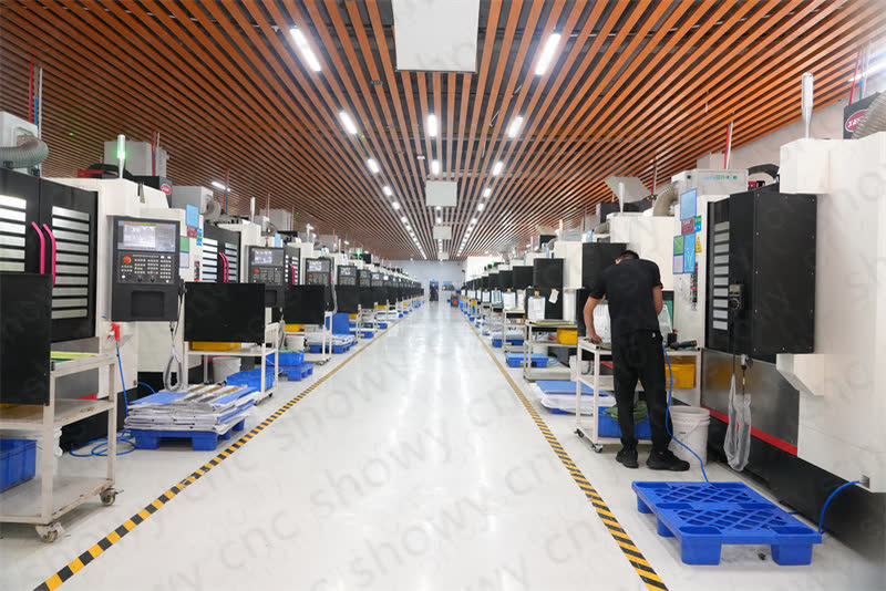
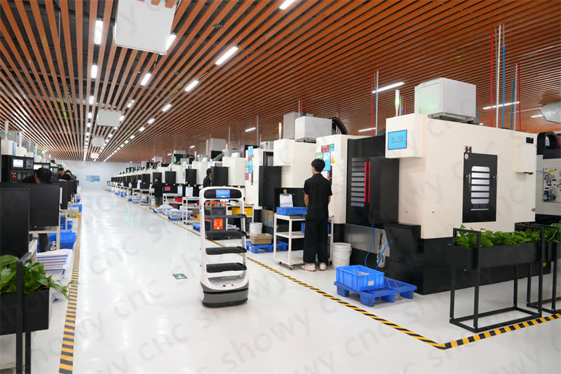
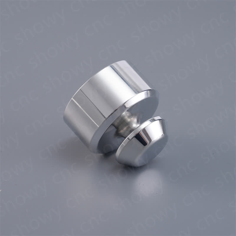
For semiconductor test jigs, precision fixtures, and micro-structural parts, our factory provides 5-axis CNC milling and turn-mill compound machining. Supports stainless steel, titanium alloy, and high-performance engineering plastics, with tolerance control of ±0.01mm and Ra0.4μm high finish, ensuring cleanliness and assembly precision.
Specifications and Machining Capabilities
The core advantage lies in GD&T control at extremely small dimensions. 5-axis coordinated machining solves challenges of deep cavities and multi-angle holes, avoiding cumulative errors from multiple clamping.
- Minimum shaft diameter 0.2mm, length-to-diameter ratio up to 1:30
- Critical mating surfaces hardness HRC50-55, wear and corrosion resistant
- Complex curved surfaces Ra0.2μm mirror effect, no chatter marks
Cleanliness and Batch Consistency
Semiconductor components are highly sensitive to surface residues. After machining, ultrasonic degreasing cleaning is performed to ensure no chips, no oil, and no metal ion residues. Through first-article inspection and full process inspection, batch appearance and dimensional consistency are guaranteed to avoid assembly interference.
- Equipped with 3D CMM and roughness meter for full dimensional inspection
- Incoming material spectral analysis, material reports provided with goods
- Independent clean packaging, anti-static and dust-proof transportation
How long is the prototyping cycle?
Standard sizes in 3-5 days, complex structures within 7 days, expedited scheduling supported to align with project milestones.
What tolerance can be achieved?
Standard tolerance ±0.01mm, critical precision mating surfaces up to ±0.01mm, specific evaluation based on drawing structure.
Send drawings to get DFM suggestions and quotes, quickly start your semiconductor component mass production plan.